
Kiselkarbid i Stockholm AB (“KISAB”) is a silicon carbide semiconductor material development and production company with operations in the tech hub of Sweden just north of Stockholm: Kista.

SILICON CARBIDE
In high-voltage power electric applications, substrate defects directly impact downstream yield and device performance.
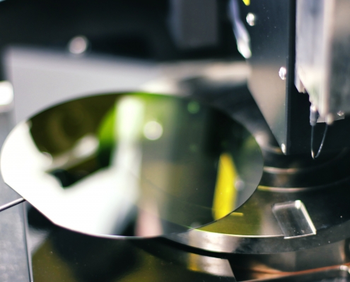
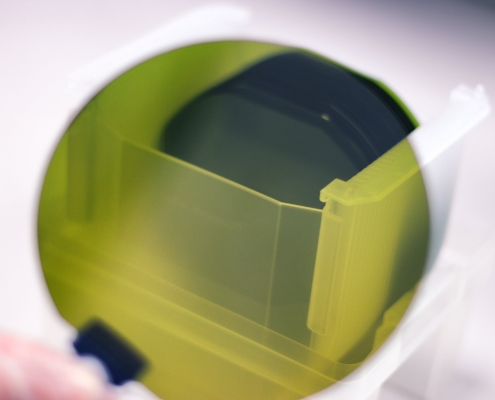
Our 8-inch wafers are grown using our proprietary Fast Sublimation Growth Process (FSGP) method to eliminate Basal Plane Dislocations (BPD), preventing power device bipolar degradation while improving yield and performance.
SILICON CARBIDE
Industry standard: Specification in line with customer demand,
Quality Standard: High purity crystal including,
Please find the data sheet of our 8-inch n-type Silicon Carbide wafers below.
SILICON CARBIDE
Industry standard: Specification in line with customer demand,
Quality Standard: High purity crystal including,
Please find the data sheet of our 8-inch n-type Silicon Carbide wafers below
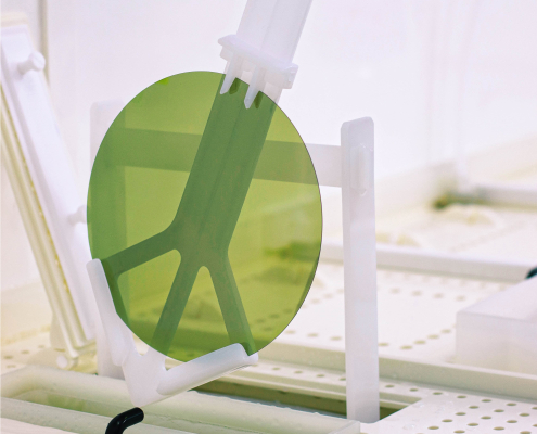
We have established a high volume production system capable of running 24/7, operated by the company’s highly qualified personnel.
The company’s proprietary process and related technologies are patented, and the production process has undergone an ISO-audit.
Kiselkarbid i Stockholm AB (“KISAB”) is a silicon carbide semiconductor material development and production company with operations in the tech hub of Sweden just north of Stockholm: Kista.