TECHNOLOGY

Kiselkarbid i Stockholm AB (“KISAB”) is a silicon carbide semiconductor material development and production company with operations in the tech hub of Sweden just north of Stockholm: Kista.

TECHNOLOGY
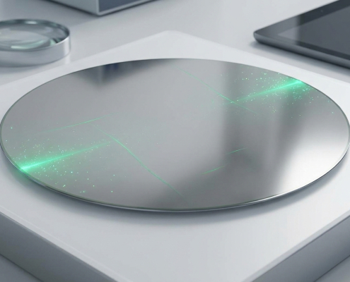
SILICON CARBIDE
The transition to 200 mm silicon carbide wafer manufacturing is bottlenecked by high crystal defect rates.
Traditional growth methods often yield Basal Plane Dislocations (BPD), which propagate into the epitaxial layer and cause bipolar degradation—ultimately leading to premature device failure in the field.
THE KISAB APPROACH
KISAB has solved this bottleneck through FSGP-M.
Our proprietary crystal growth approach produces 200 mm SiC substrates that are free from BPDs.
By addressing defects at the substrate level, we ensure maximum reliability for the epitaxy and device fabrication stages that follow.
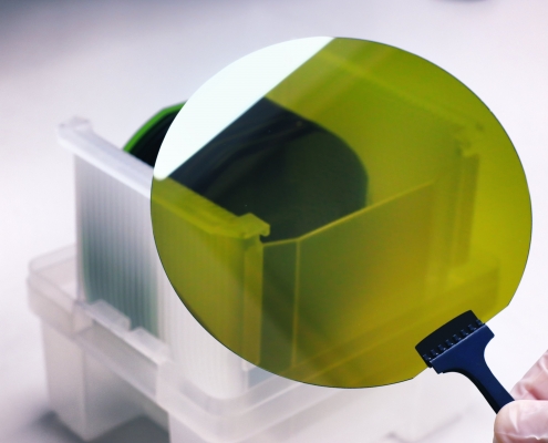

IMPROVEMENT
High-quality substrates are the foundation of reliable power electronics.
Our defect-free growth enables higher yields for device manufacturers and uncompromised performance for the end-user.
FURTHER READING
Access further technical insights including an introduction to the material silicon carbide, bipolar degradation and how it causes device failure, and features of FSGP-M grown wafers.
Kiselkarbid i Stockholm AB (“KISAB”) is a silicon carbide semiconductor material development and production company with operations in the tech hub of Sweden just north of Stockholm: Kista.